THIS IS AN INCOMPLETE MIRROR
Please check the "Home" link below for the original website.
This is a mirror of the construction details only. See Kees Cook's
modified 27c801 build
instructions for faster read and write times with code for Linux.
27c801 EPROM Programmer Project
This project is based on EPROMr 2.0, (C) Copyright 1998 Lewin A.R.W. Edwards. Lewin A.R.W. Edwards can be contacted at sysadm@zws.com, http://www.zws.com, or by telephone at (+61) 412 809805
Overview - Tools - Schematic - Parts List - Construction - Links
The objective of this project was to produce a simple and cheap EPROM burner.
I was familiar with Lewin Edwards' EPROMr2 project, a parallel port EPROM burner controlled by software running under DOS. The burner did not have support for the 27c801, however, so I set about modifying the burner and software in order to support this device. For the purposes of this tutorial, I decided to produce a simplified version of the burner and software exclusive to the 27c801 EPROM. The burner is built on Veroboard and can be constructed very cheaply - typically less than £15 for all of the parts. Read on...
Tools (and other things) you'll need
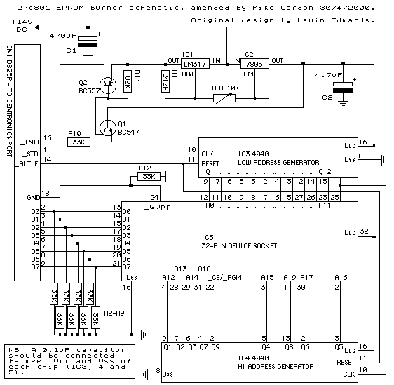
Here's the schematic (circuit diagram) for the burner you're going to build. If you don't understand what the symbols mean, don't worry! I'll go through the construction stages step by step.
Note: I've specified a standard socket for the EPROM, Maplin KW69A, to keep the cost of the burner down. A 32-pin ZIF socket, such as Maplin JK75S, will add around £10 to the cost of your burner but will greatly simplify inserting and removing EPROMs. You could always build the burner with a standard socket, then plug a ZIF socket into it at a later date if you want!
Component |
Qty. |
Maplin Code |
Maplin Price (ea.) |
Total Price |
|---|---|---|---|---|
| Strip Board, 39 strips x 62 holes | 1 | JP50E | 1.95 | 1.95 |
| BC547 Transistor (Q1) | 1 | QQ14Q | 0.06 | 0.06 |
| BC557 Transistor (Q2) | 1 | QQ16S | 0.07 | 0.07 |
| 16V 4.7uF Tantalum Capacitor (C2) | 1 | WW64U | 0.25 | 0.25 |
| 35V 470uF Electrolytic Capacitor (C1) | 1 | VH47B | 0.37 | 0.37 |
| 50V 0.1uF Ceramic Disc Capacitor | 3 | BX03D | 0.12 | 0.36 |
| SIL Resistor 47k ohm (R2 - 9) (parallel with 100k to give 33k) | 1 | RA31J | 0.14 | 0.14 |
| SIL Resistor 100k ohm (R2 - 9) (parallel with 47k to give 33k) | 1 | RA32K | 0.14 | 0.14 |
| Metal Film Resistor 33k ohm (R10, 12) | 2 | M33K | 0.06 | 0.12 |
| Metal Film Resistor 82k ohm (R11) | 1 | M82K | 0.06 | 0.06 |
| Metal Film Resistor 240 ohm (R1) | 1 | M240R | 0.06 | 0.06 |
| 10k ohm horizontal linear preset (VR1) | 1 | UH03D | 0.18 | 0.18 |
| LM317 variable voltage regulator (IC1) | 1 | RA87U | 0.42 | 0.42 |
| 7805 +5 volt regulator (IC2) | 1 | AV16S | 0.67 | 0.67 |
| 4040 12 bit binary counter IC (IC3, 4) | 2 | QW27E | 0.84 | 1.68 |
| 16 pin DIL IC socket (for the 4040s) | 2 | BL19V | 0.16 | 0.32 |
| 32 pin DIL IC socket (for the EPROM) (IC5) | 1 | KW69A | 0.59 | 0.59 |
| 2.1mm power connector | 1 | RK37S | 0.42 | 0.42 |
| 25 Pin D-type plug connector (CN1) | 1 | FG68Y | 0.98 | 0.98 |
| Total (excluding VAT) | 8.84 | |||
| Total (including VAT) | 10.39 |
The parts list is for the burner itself and does not include a mains adaptor. Any universal plug-pack unregulated supply with 12 volt selectable output will do - these are typically available from market stalls and cheapie Poundstretcher type shops for around £4, as well as from your local friendly electrical retailer for a slightly larger sum!
Another necessity is a parallel port extension cable for actually connecting up the burner - this will have a 25 pin plug on the PC end, and a 25 pin socket on the other end. If you have a flatbed scanner which connects to the parallel port, chances are you already have such a cable - if not, it shouldn't cost more than a few pounds from a computer shop or computer fair. I have had some reading/burning problems with long cables - make sure the cable is less than a metre long. Anything longer and you could run into difficulties.
For the PC, you'll need at least a 386 with 4 Megabytes of RAM, running MS-DOS (or equivalent), Windows 95, Windows 98, or OS/2. To read and write EPROMs, the parallel port should support one of the bi-directional protocols - look for EPP or similar in your BIOS setup, and make sure it's enabled. If your parallel port doesn't have bi-directional capability, you may find that you can't read EPROMs, although burning should work fine.
These are the parts you should have:
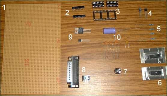
Veroboard
SIL Resistors
IC Sockets
Transistors
Metal Film Resistors
ICs (4040 Counters)
Horizontal Linear Preset (variable resistor)
Connectors
Voltage Regulators
Capacitors
Now to construct the burner, step by step.
Step One - Cutting And Marking The Veroboard
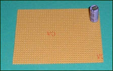
The EPROM burner is constructed on Veroboard, a thin SRBP or fibreglass board with holes 0.1 inch apart, and copper tracks linking the holes in rows on one side of the board. This allows circuit connections to be made quickly and easily. From now on I'll refer to the track side of the board, which is the side of the board with the copper tracks, and the component side, which is the blank side on which the electronic components are mounted. (In the photo above, the board is shown component side up.)
Before we can begin using the Veroboard we need to cut it to the appropriate size. We also need to mark the holes and tracks with numbers and letters so we know where we are to mount the components.
The burner is to be built on a piece of board 39 tracks wide, with 30 holes per track. Count 30 holes down in the direction of the tracks then score the Veroboard across at right angles to the tracks, using a Stanley knife and ruler. (See picture). Break the board at this point. (Careful now!) If you've scored the board properly you should get a clean break.
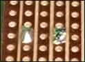
The next thing to do is lay the board down on a piece of paper, track side up. Trace all around the board using a pencil, and mark the positions of the tracks using letters, and the positions of the holes using numbers. Assuming the tracks are running in a vertical direction, start at the top right corner and label the tracks A to Z from right to left. You've run out of letters, so use the designation AA to AM for the remaining tracks. Now, starting in the top right hand corner, label the holes from 1 to 30 down the right hand side of the board. Look at this picture to see how it's done - the markings must be exactly in the positions shown.
Now TURN THE BOARD OVER so the component side is facing up, as in this picture. This gives us a reference for the co-ordinates of each hole on the board, and I will be referring constantly to this throughout the guide. To read off the correct hole, just put the board back on the paper again and line up the markings, making sure the board is COMPONENT SIDE UP and that the orientation is the same each time. For example, the hole at the top right hand side of the board in this picture is 1A, the one to the left of it is 1B and the one below it is 2A.
Step Two - Building The Power Supply
Now we can start adding some components. We'll start with the power supply. As mentioned previously, the burner is powered by a 12v universal unregulated mains adaptor; the supply from this has to be smoothed and regulated before it can be fed to the ICs on board the burner. We'll also add the transistors which switch the programming voltage on and off.
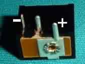
C1 on the schematic is a 470uF (470 microfarad) electrolytic capacitor. The output of the mains adaptor is likely to be somewhat rough, so we add this capacitor to smooth it out. It looks something like this:
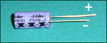
Electrolytic capacitors are polarised - that means they have a positive and a negative lead, and must be connected the right way round. The negative lead is slightly shorter than the positive, and is usually marked by a series of minus signs down the side of the capacitor body. The positive lead is sometimes identified by a plus sign, but it's usually unmarked.
You need to solder the positive lead of the capacitor into hole 7D, and the negative lead into 7B. Push the leads all the way in, so the capacitor sits flush with the component side of the board. Bend the leads outward slightly so the capacitor stays in place. Solder both leads on the track side and trim the excess with your wire cutters. Here's the finished result -
Now we can add some more components. Next to go on are the voltage regulators; a 5 volt regulator, 7805, and a variable regulator, LM317. This picture shows what they look like, along with the lead designations. Note that the regulators in this picture look different - the 7805 is in a P1d package, while the 317 is in a smaller TO92s package. You might come across a 317 regulator in a P1e package which looks similar to the 7805 in the picture; the pin designation is the same as for the TO92s package, however, and for this design it doesn't matter which you use.
For the 7805, Pin 1 goes to 13D, Pin 2 to 12B, and Pin 3 to 11C. You'll need to bend the pins a little so they reach the holes.
For the LM317, Pin 1 goes to 15F, Pin 2 to 15E and Pin 3 to 15D.
C2 on the schematic is a 4.7uF tantalum capacitor - basically a miniature electrolytic capacitor, so it is polarised. The positive lead is indicated by a stripe, dot or plus sign on the capacitor, as shown below.
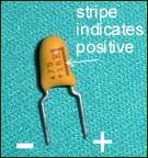
Connect the positive lead to 16C, and the negative lead to 14B.
Next, two resistors - a 240 ohm, R1, and an 82k (82,000) ohm resistor, R11. Here's the resistor markings and what they mean.
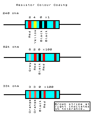
Connect the 82k resistor between 23E and 27F, and the 240 ohm resistor between 14E and 10F. Resistors aren't directional; it doesn't matter which way round they go.
The next component is a 10k ohm variable resistor, also known as a trimpot or preset, VR1. This is what it looks like.
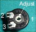
The control in the centre of the trimpot is adjusted using a small screwdriver and is used to determine the resistance between pins 1 and 2 and/or pins 2 and 3. We will adjust the trimpot later in order to set the programming voltage, but don't worry about it for now.
Pin 1 goes to 19B, 2 goes to 18F, and 3 to 20F. The trimpot should be a perfect fit, i.e. you shouldn't need to bend the pins.
The final two components in this section are bipolar transistors. Q1 is an NPN transistor, BC547. Q2 is a PNP transistor, BC557. This picture shows the pin designations.
For Q1 (BC547), connect the emitter to 29E, base to 27C, and collector to 28F. For Q2 (BC557), connect the emitter to 22E, base to 22F, collector to 22G. These transistors switch the programming voltage on and off, so it's important they're connected correctly. I'll explain more about this in the Testing section.
The final thing we need to do in this section is cut some tracks using the track cutter mentioned earlier. You need to cut the following holes: 19F, 21F and 24E. Place the cutter (or drill bit) in the appropriate hole on the track side, apply light pressure and rotate clockwise until the copper all around the hole has been removed. (The idea is to break the circuit connection at this point, so make sure all the copper is gone on both sides of the hole.)
That's it! Now onto the next step.
Step Three - The Logic Section
The logic section consists primarily of the 4040 ICs, the EPROM socket, and the (many!) connections between them. We'll start by soldering on the two 16 pin IC sockets, for the 4040 counter chips. This picture shows the pin designation. Note that the sockets are symmetrical (they will go either way round), so a notch or indentation is present at one end of the socket to show which way it's supposed to go. A corresponding notch is present on the chips themselves.
Why use a socket? Why not just solder the 4040s directly to the board? The 4040 chips use CMOS (Complementary Metal Oxide Semiconductor) logic which is very vulnerable to static electricity, so it's best to handle the chips as little as possible. Also, if you heat up the chips too much with your soldering iron it could damage them. So we solder a socket to the board instead, and insert the chips into them at the very last stage of assembly.
The first 4040 is IC3, the low address generator. Basically the 4040s output a value which points to a particular location (address) within the EPROM. This value starts at zero and increments by one every time it receives a clock signal from the parallel port. This allows us to read or write the data inside each memory location in the EPROM, via the EPROM's data lines which are connected to the PC via the parallel port. A single 4040 IC can only count up to 4095 (FFF in hexadecimal); we need two of them to cover the full address range of the EPROM. (FFFFF in the case of the 27c801, giving us 1048576 bytes or 1 Megabyte.)
Anyway, align the socket so that pin 1 goes to 10J, and pin 16 goes to 13J. Solder all the pins.
The second 4040 is IC4, the high address generator. Pin 1 of this goes to 19J, Pin 16 to 22J.
Now take out your track cutter and cut the following holes: the 8 holes from 11J through 11Q, 8 holes from 20J through 20Q, 8 holes from 16J through 16Q; 24 holes in all.
We'll leave the 32-pin EPROM socket for now, because we need to route wires under it. (Well, we don't have to, but it looks neater if we do!) Bear in mind when routing wires that the EPROM socket will eventually be situated such that Pin 1 goes to 13U and Pin 32 goes to 19U, so don't let any wires cross the points where the pins go in.
33k ohm resistors are used as pull down resistors on the data lines. We can implement this using two SIL resistors, a 44k ohm and a 100k ohm, in parallel - this is a lot less hassle than using discrete metal film or carbon resistors. SIL resistors consist of 8 resistors in a single package with a common ground. The common (Pin 1) is marked with a spot on the case, as shown below.
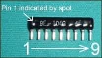
The resistor in the picture is the 100k ohm, by the way. Since the two resistors are paralleled anyway it doesn't matter which goes where. Put in one of the resistors so that Pin 1 goes to 8AJ and Pin 9 to 8AB. Put in the other resistor so that Pin 1 goes to 9AJ and Pin 9 to 9AB.
Get out your wire cutters and strippers, and solder wire links between the following pairs of holes:
30B and 30S
29C and 29R
29S and 29AK
8Q and 8S
17Q and 17S
14J and 13R
23J and 22R
18U and 18R
14AJ and 14S - keep this straight and flush with the board.
29G and 29AC
Solder a 33k ohm resistor between 28AK and 28AC. See the resistor colour coding diagram further up the page.
Now to add the final three capacitors. These are 0.1uF ceramic capacitors, for decoupling, and look like this.
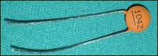
They are non-polarised so it doesn't matter which way round you put them. Solder one between 9Q and 7R, another between 18Q and 16R, and the third between 20U and 20S.
Now we'll add the data lines - some more wire links.
7AB to 20AJ
7AC to 20AI
7AD to 20AH
7AE to 20AG
7AF to 20AF
Then cut tracks at 10AB, 10AC, 10AD, 10AE, 10AF.
We can add some of the address lines and other lines now. Wire links:
15T to 15O
18N to 15W
29N to 29AE
14Q to 11AF
9P to 11AE
9O to 11AD
7N to 11AC
7L to 11AB
8K to 11AA
7M to 12Z
14M to 12Y
14N to 20Z
14L to 20AA
14K to 20AD
23Q to 14X
18P to 20Y
18O to 20X
18L to 14V
18K to 20W
18M to 20V
23M to 14U
8J to 20AB
28T to 28O
24P to 9J
Now solder on the 32 pin EPROM socket, so pin 1 goes to 13U and pin 32 goes to 19U.
Cut tracks at holes: 16U through 16AJ inclusive. (16 holes in all.)
Connect the last 33k ohm resistor between 26E and 26A.
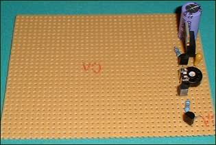
That's it for this step: this picture shows the story so far!
Step Four - Connecting The Connectors
The final stage involves connecting up the power and parallel connectors and gluing them to the board. This picture shows the pin numbering for the parallel connector. Use wire links to connect them to the appropriate holes on the board, as follows:
Pin 1 to 15P
Pin 2 to 5AG
Pin 3 to 5AH
Pin 4 to 5AI
Pin 5 to 5AB
Pin 6 to 5AC
Pin 7 to 5AD
Pin 8 to 5AE
Pin 9 to 5AF
Pin 14 to 4T
Pin 16 to 4A
Pin 18 to 5AJ
This is the pin designation for the power connector:
Use wire links to connect the positive (+) lead to 5D, and the negative (-) lead to 5B.
Now use glue to mount the connectors at the top edge of the board, with the actual connectors themselves facing backwards. Mount them upside down so that the pins are sticking up in the air. Allow the glue to dry.
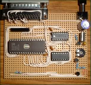
Now you need to be very careful - touch a grounded point (such as a radiator) or wear an anti static wrist strap. Don't wear nylon clothing as this can hold a static charge. (These precautions apply to handling EPROMs as well.) Carefully remove each 4040 IC from its protective packaging and insert them into the sockets on the board. Make sure the notch on the chip lines up with the notch on the socket. (Obviously it does not matter which chip goes in which socket, as they are both the same!) Now your burner is built and you're ready to test it out! See a picture of the finished article.
EPROM Programmer Discussion Forum - discuss issues related to EPROMs and programmers.
Data sheets for 27c801 and 27c080 EPROMs.
This page maintained by Mike Gordon. Last updated 24th January 2001.
DISCLAIMER: The information on this page is true to the best of my knowledge, but I make no guarantees, etc, etc. I accept no responsibility for any harm which may occur as a result of using this device to burn the firmware for a life-support machine, a nuclear submarine, or the first manned mission to Mars. Opening up your Samsung 709 will invalidate your guarantee, and will probably make your hair fall out too. Don't say I didn't warn you.